Graphene-Based COVID-19 Biosensor Development at UPenn
I engaged in two summers of research (2022 and 2024) with Dr. Charlie Johnson at the University of Pennsylvania. Working with PhD candidates Inayat Bajwa and Olivia Dickens, I helped develop graphene-based, field-effect transistors for rapid COVID-19 detection. In addition to product design and experimentation, my research involved extensive review of scientific literature, weekly presentations, and knowledge of nano-fabrication techniques.
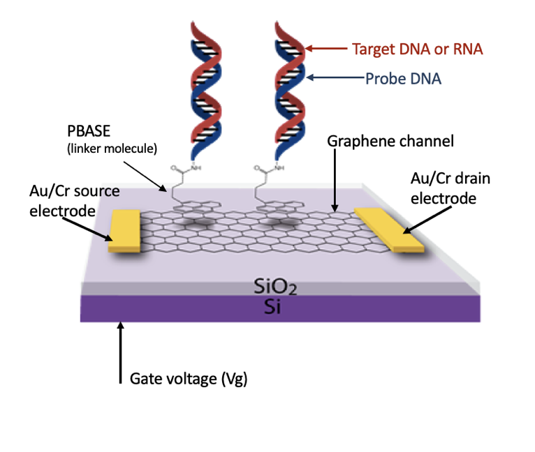
The Johnson Lab leverages the unique physical and electronic properties of graphene, a 2D and highly-conductive material, for biosensing applications. The lab originally developed graphene-based sensors to detect HIV-1, and during my time in the lab, we adapted similar designs to detect COVID-19.
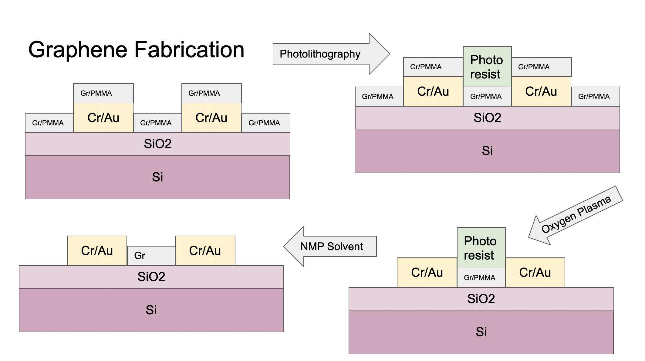
The development and fabrication of graphene field-effect transistor (GFET) devices followed a multi-step process:
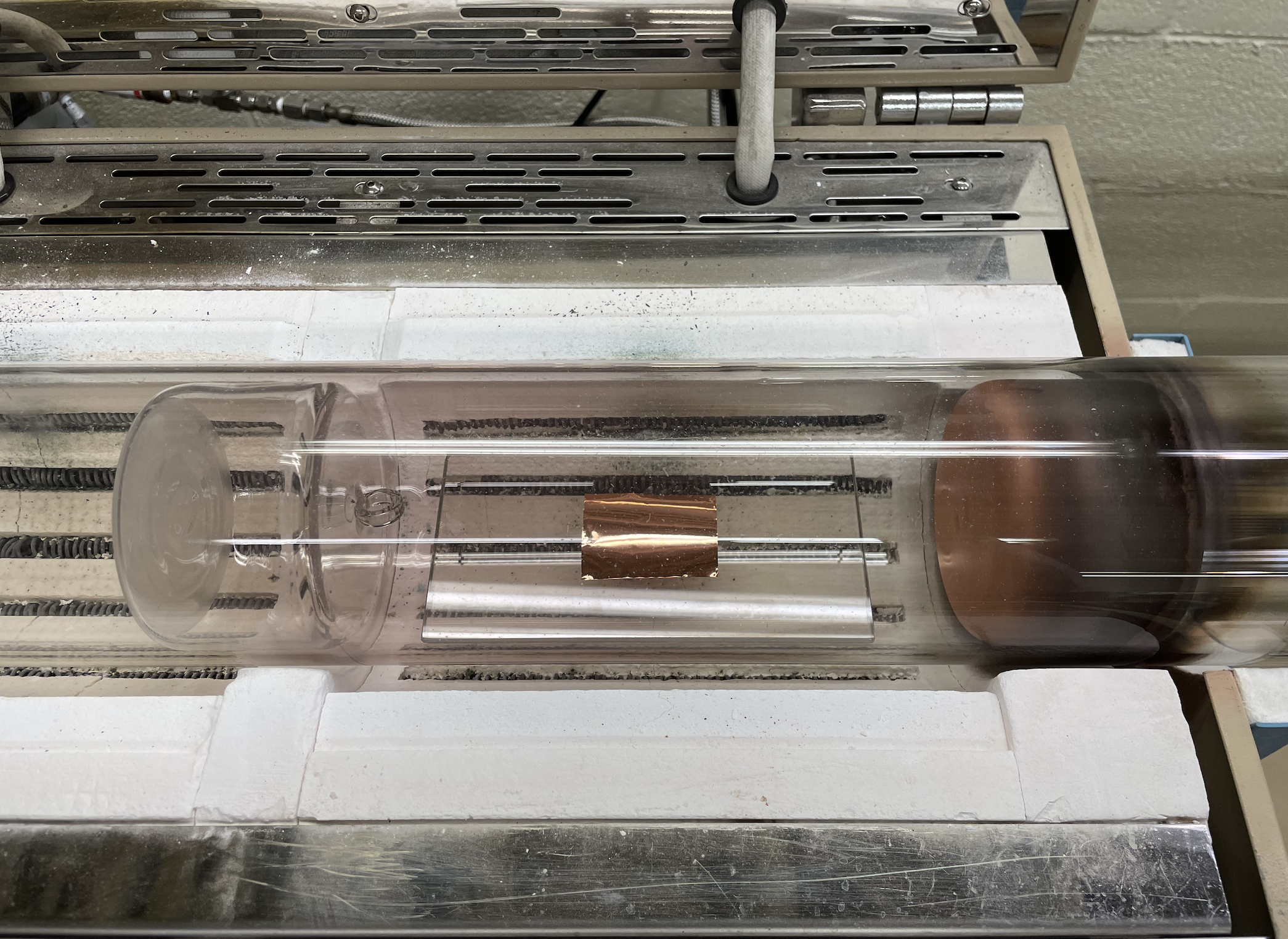
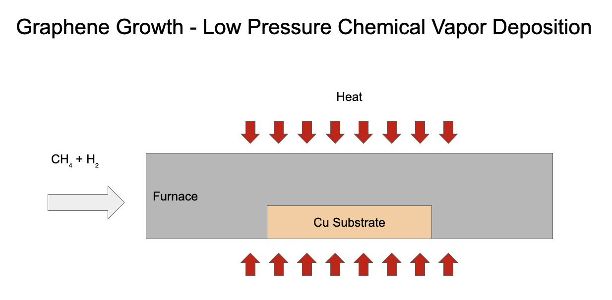
Graphene growth on a copper substrate using low-pressure chemical vapor deposition (CVD)
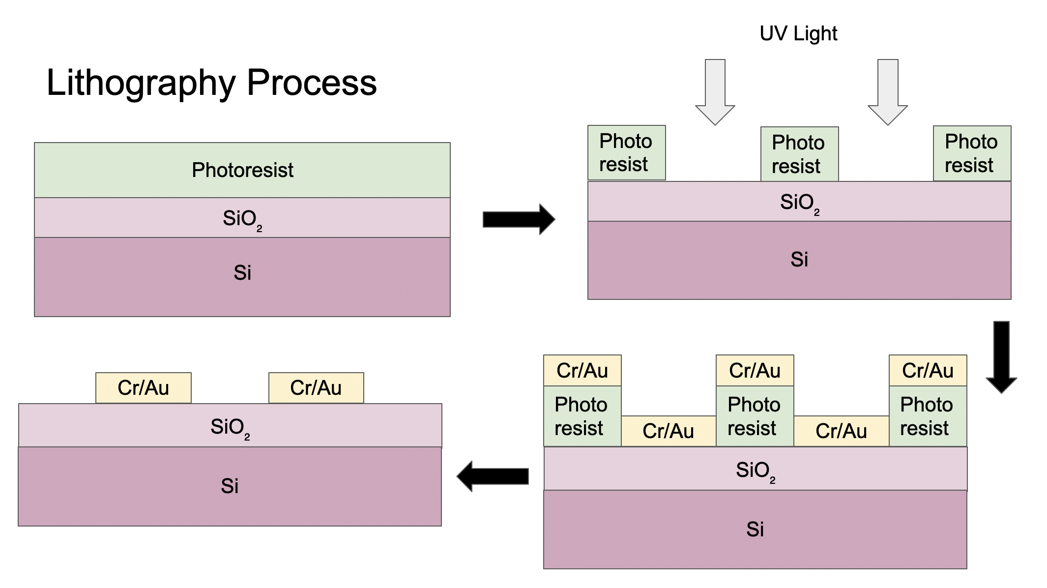
Chromium and gold thin-film deposition on a silicon oxide wafer via photolithography
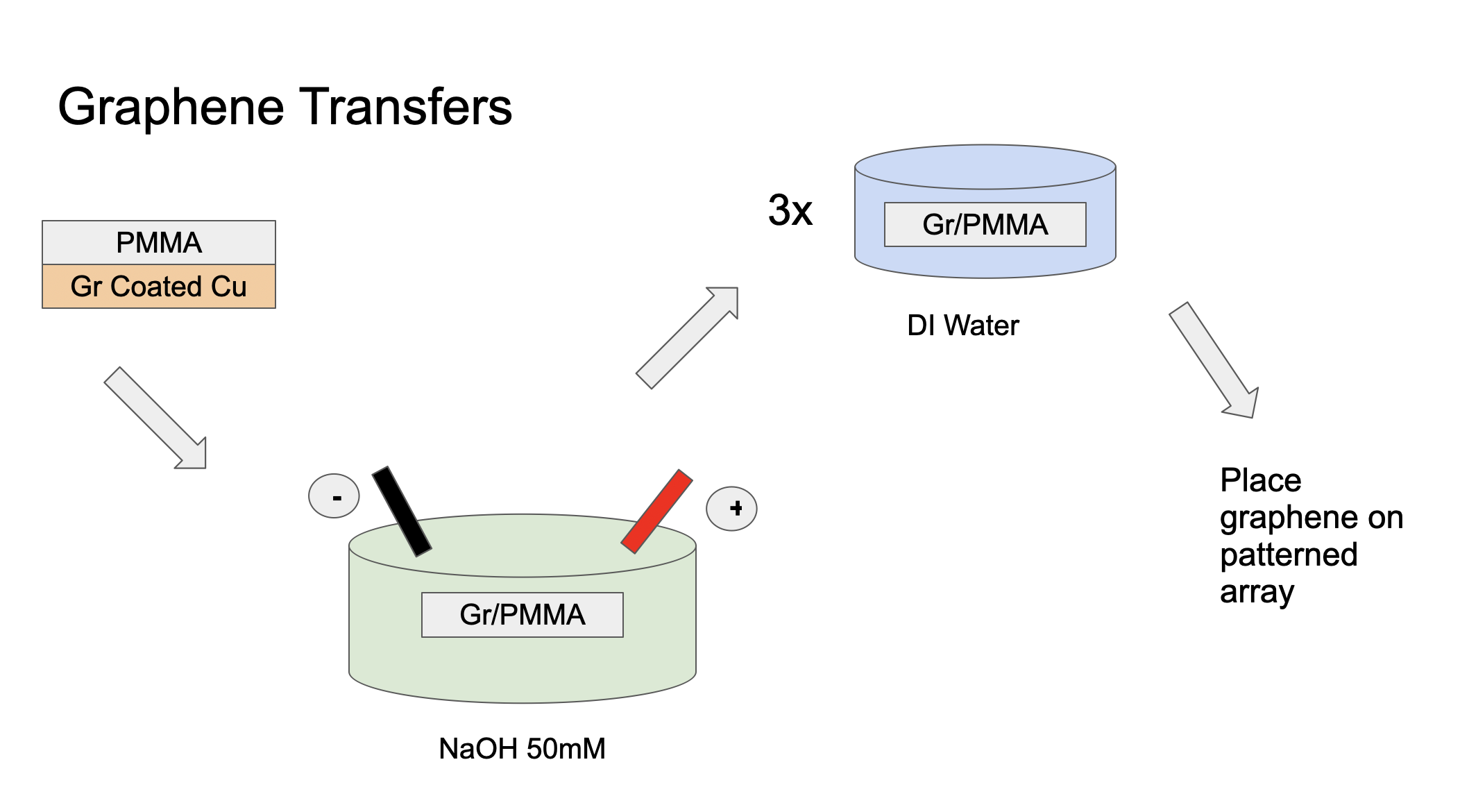
Graphene and polymethyl methacrylate (PMMA) transfer to device chip with an electrolysis-based “bubble transfer” method
PMMA removal through a second photolithography process
Chip exposure to target molecules
Electrical characterization of devices through Dirac voltage shift analysis
GFET Project Summary
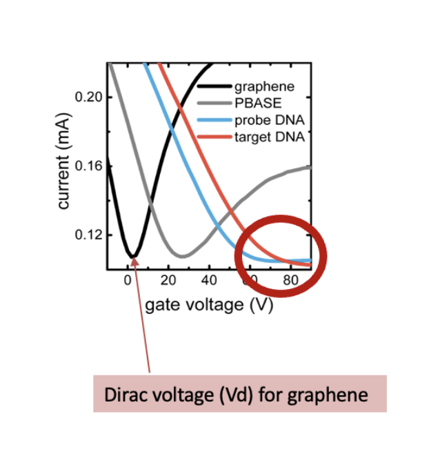
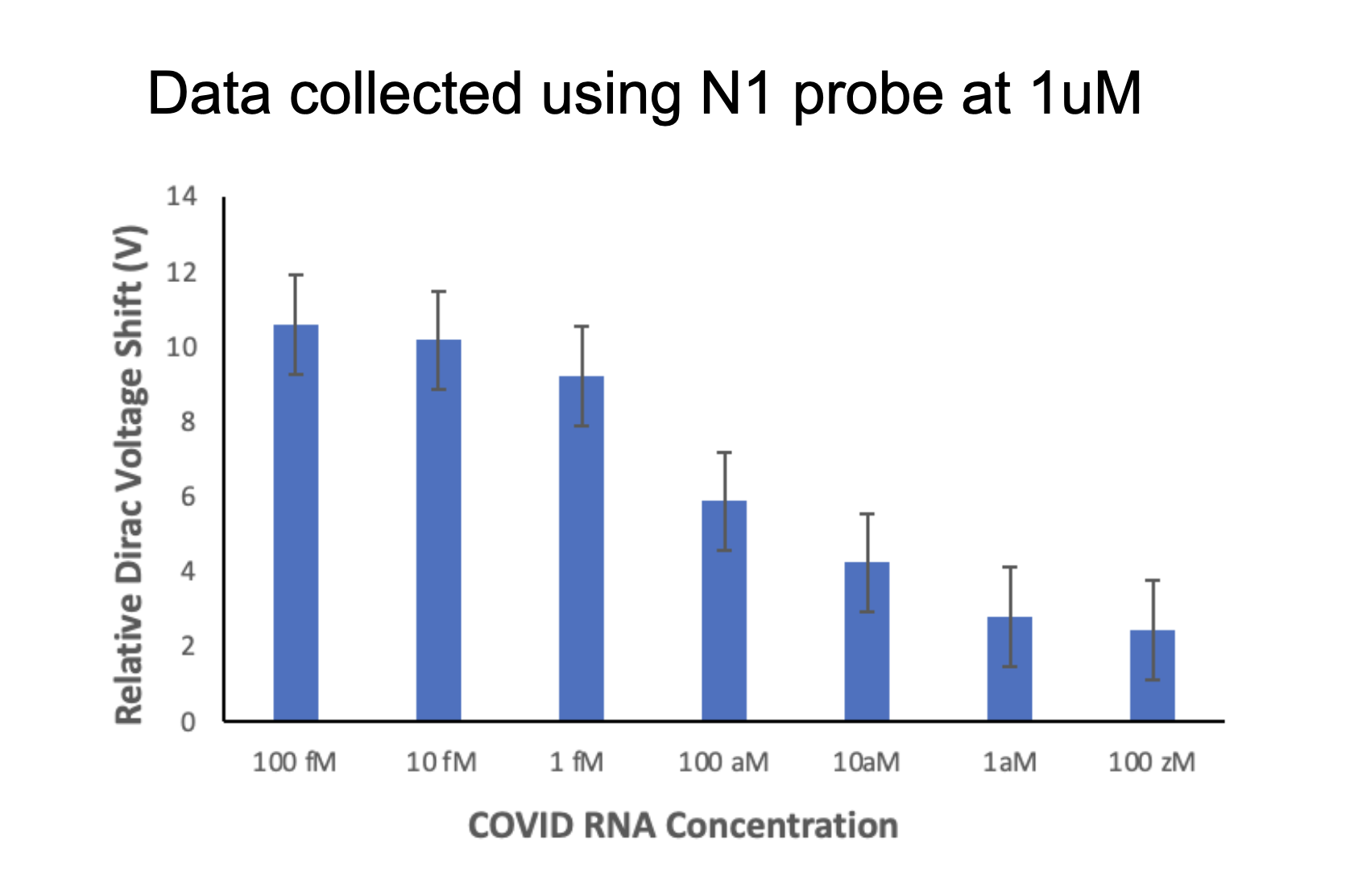
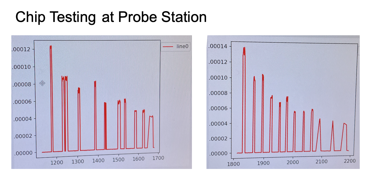
We investigated the relationship between COVID-19 mRNA concentration and the corresponding Dirac voltage shift of the device. The sensors demonstrated a lower limit of detection of 100 zeptomolar, highlighting the high sensitivity and efficiency of the system.
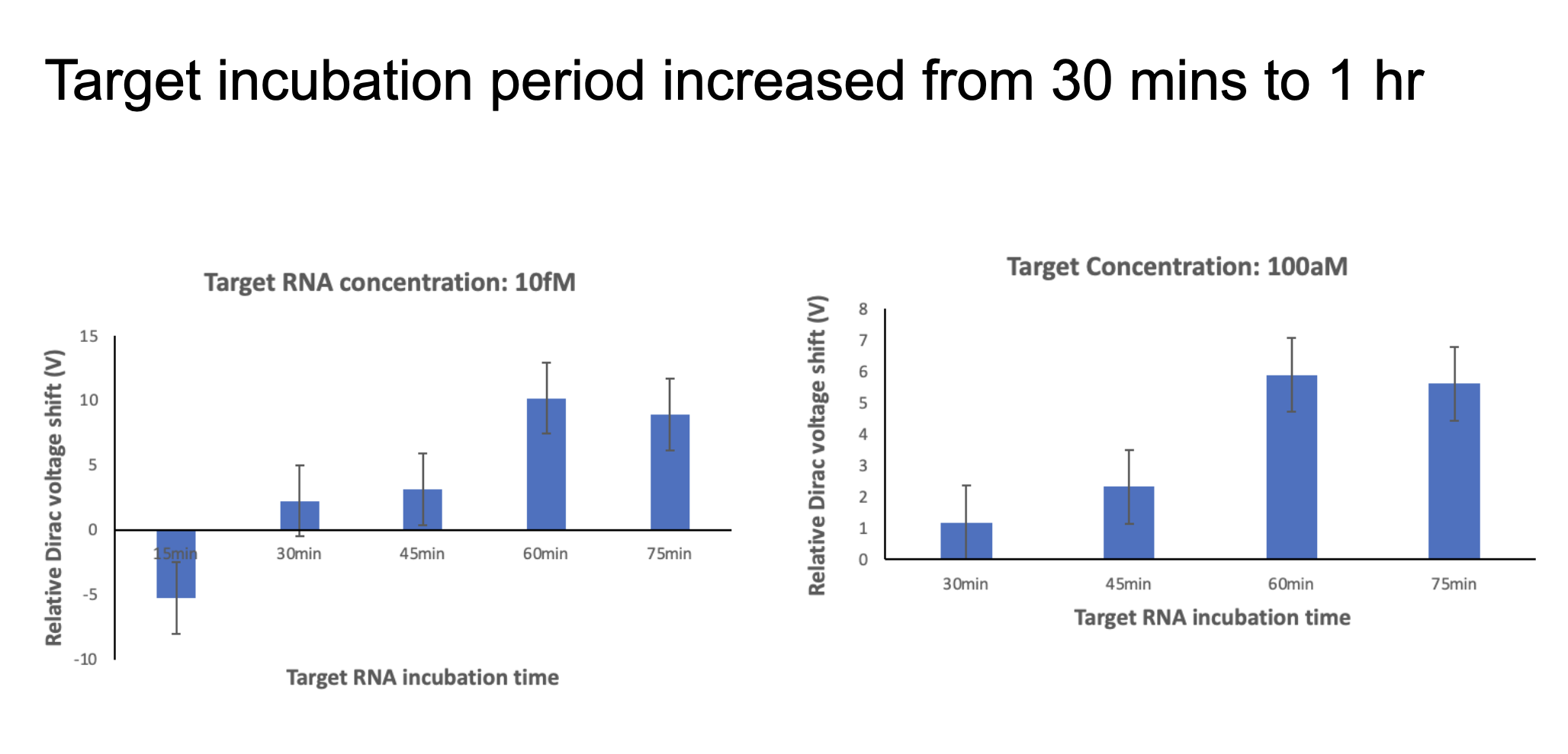
Using two different concentrations of the target mRNA, we also tested the effect of incubation time with the 20mer probes. The results show a saturation in the signal at about one hour, which informed our decision to standardize the target incubation time to one hour for subsequent experiments.
GFET Results
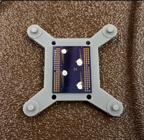
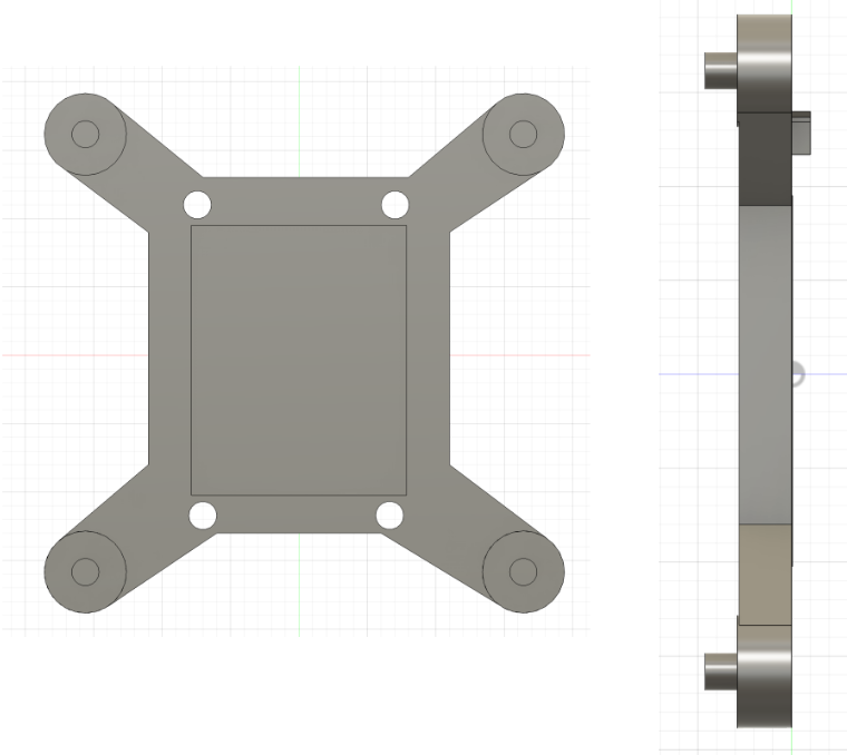
With SolidWorks, I designed and 3D-printed custom lids for portable COVID-19 testing devices as shown in the figures to the right. Precise chip alignment was critical to ensure reliable probe contact with the chip electrodes. Samtec connectors connected the chip electrodes to the circuit board. The circuit board was connected to the probe station.
The lid design incorporated four snap-fit posts that aligned with corresponding holes on the circuit board, securely positioning the Samtec connectors between the chip and the board to maintain consistent electrical contact.
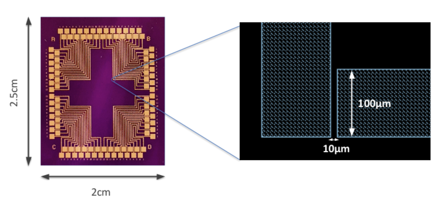
In addition, I used Layout Editor to contribute to the chip mask design for the metal deposition photolithography process, learning more about the fundamentals of microchip fabrication and device layout.
Chip Design and Fabrication Projects
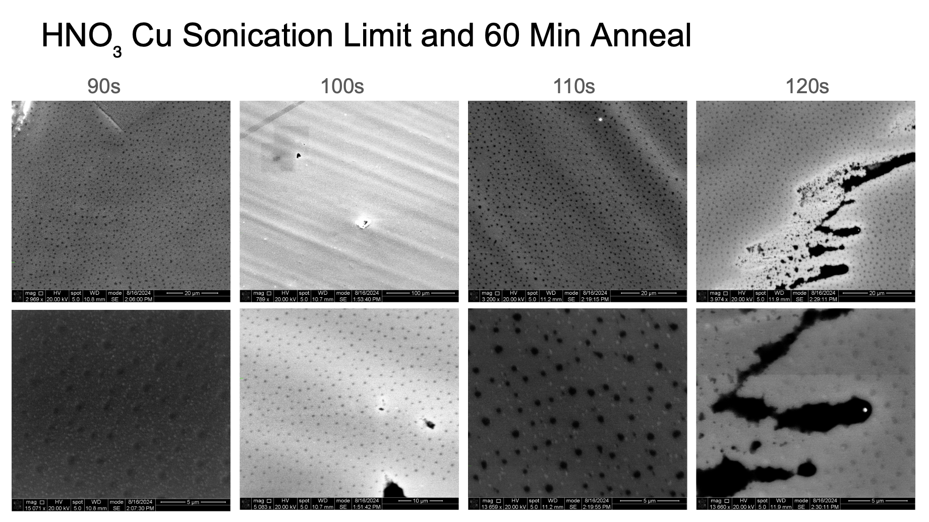
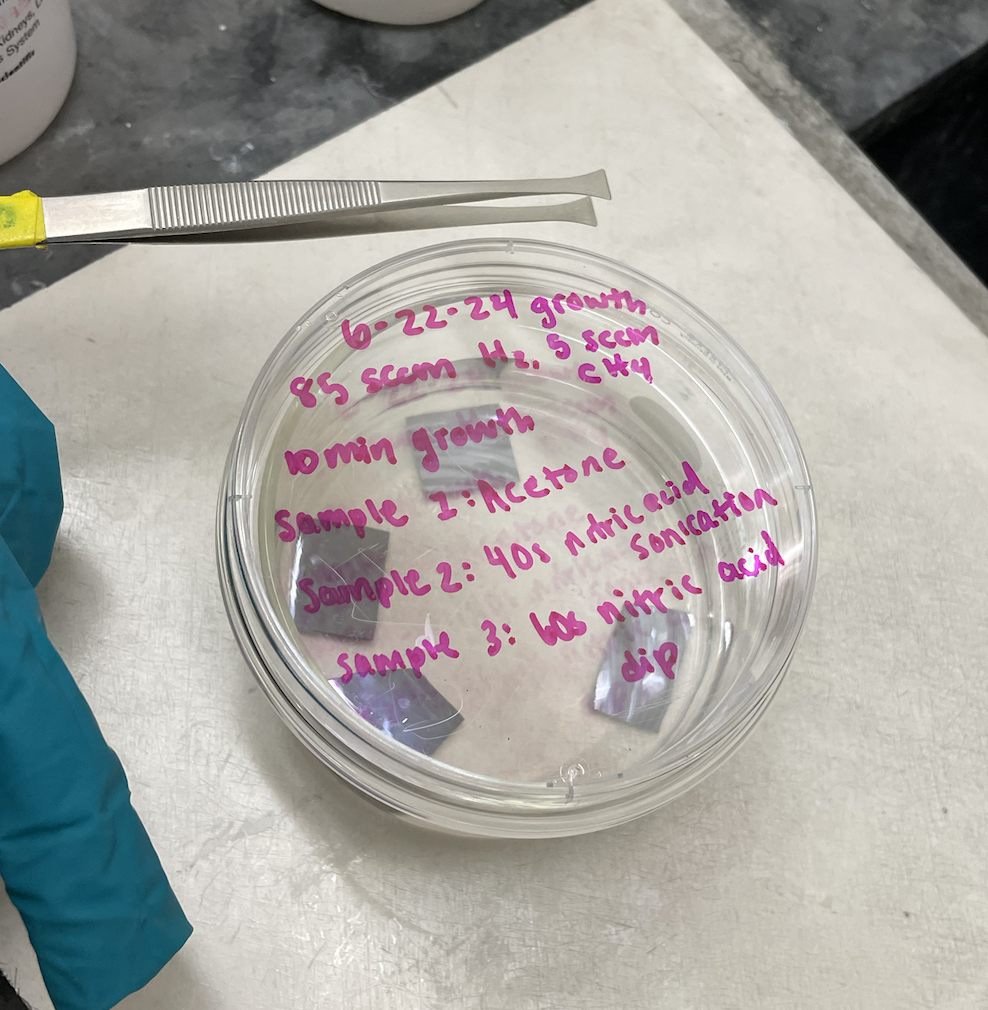
I optimized the lab’s graphene growth protocol to reduce material impurities and structural defects. Growing graphene on a copper substrate is an unpredictable process because differences between copper rolls can significantly impact graphene quality. However, prior research indicates that defects can be minimized through the careful optimization of copper surface preparation and gas flow conditions during CVD.
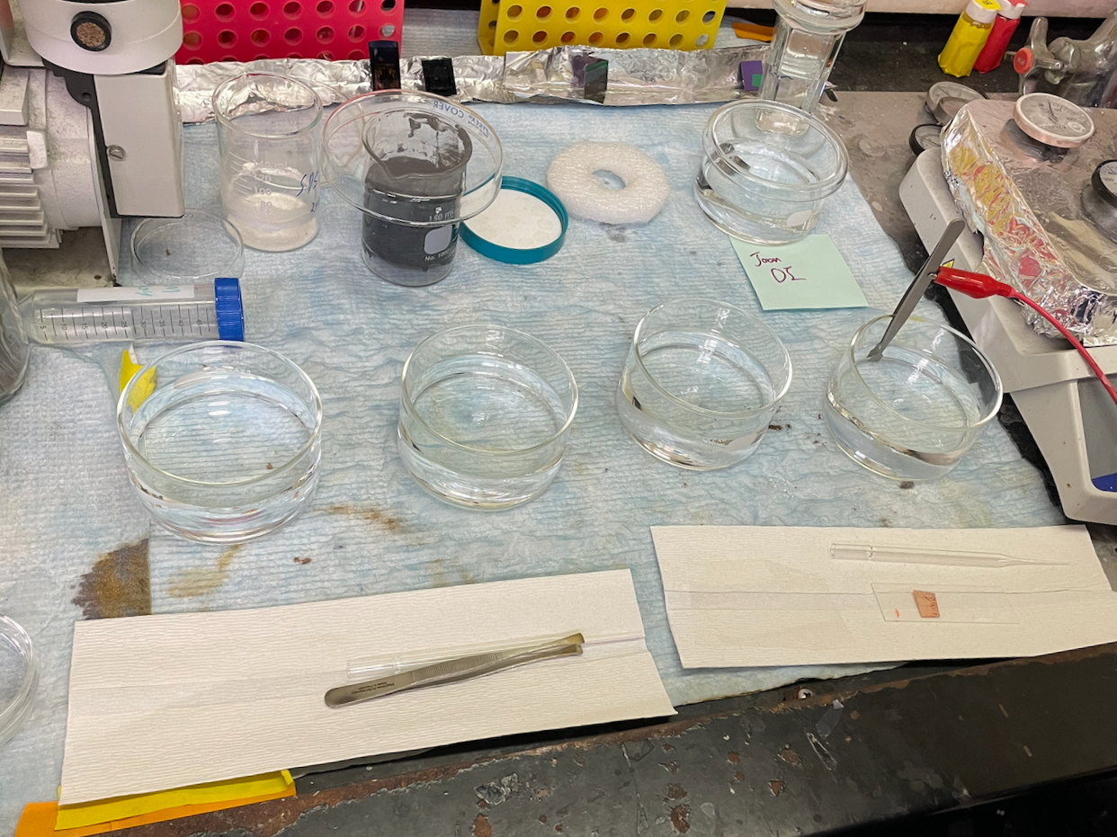
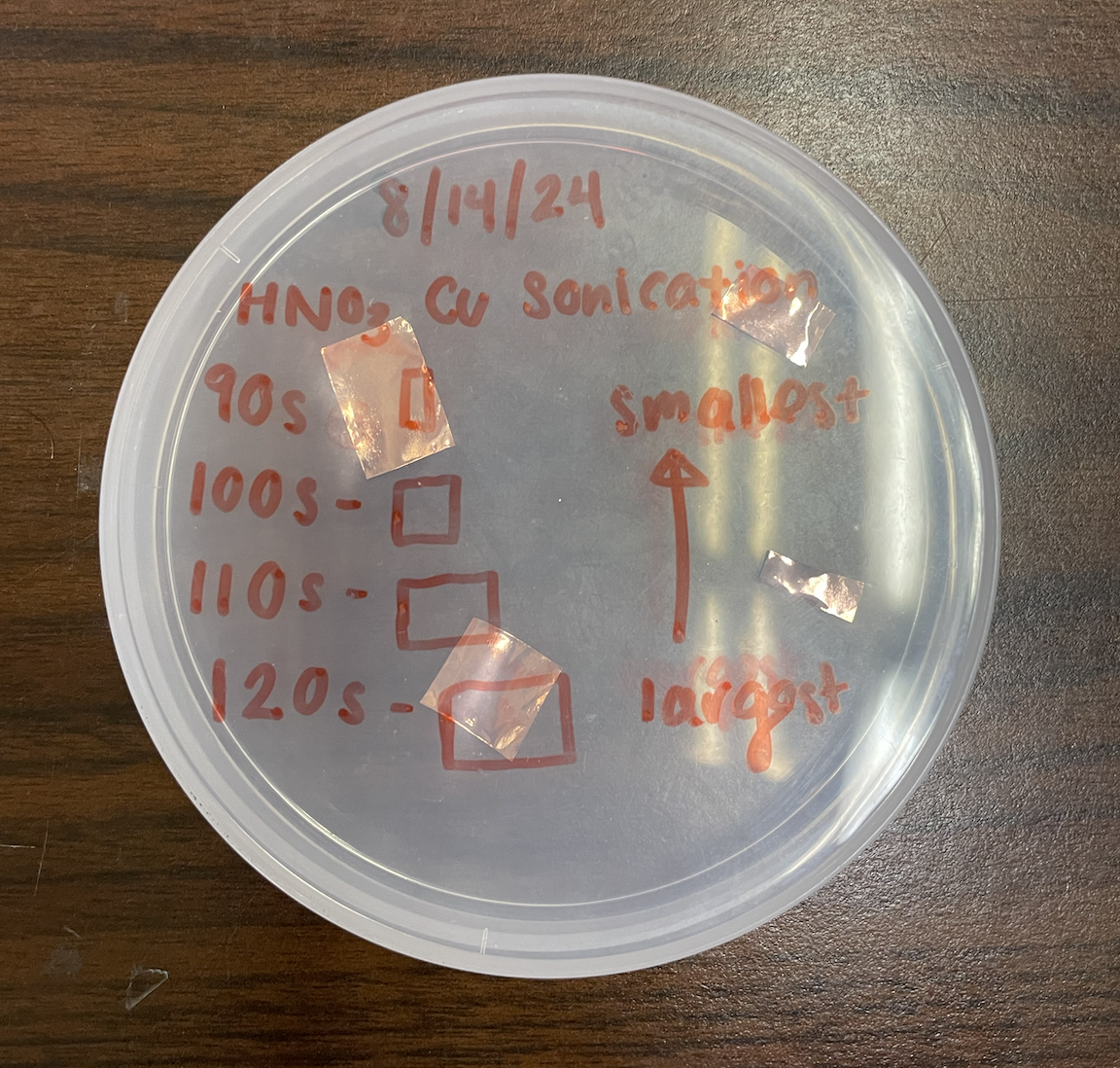
To address this variability, I systematically tested multiple copper cleaning methods. With different cleaning products (isopropyl alcohol, acetone, and nitric acid), I used both dip and sonication techniques for varying durations. I also evaluated the effect of annealing time during growth.
Graphene quality was assessed using scanning electron microscopy (SEM), which revealed an optimal protocol of a 60-second nitric acid treatment followed by a 60-minute anneal.